
The rapid evolution of wearable technology and Internet of Things (IoT) devices is driving demand for chips that are not only smaller but also more energy-efficient and powerful. Traditional semiconductor designs, constrained by horizontal layouts, struggle to meet these demands. Erik Hosler, a thought leader in semiconductor packaging and IoT innovations, emphasizes how 3D integrated circuits (3D ICs) are enabling breakthroughs in performance and miniaturization, transforming the landscape of wearable and IoT technology.
Smaller Footprints with Enhanced Capabilities
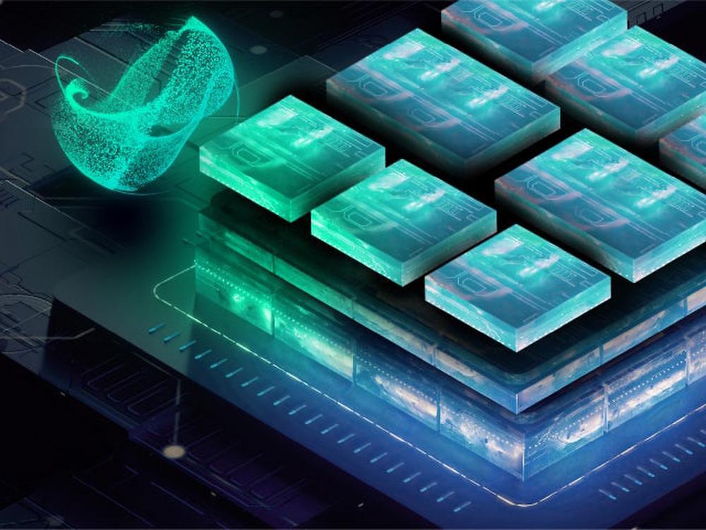
Space is a premium in wearable and IoT devices, where compactness is critical. 3D ICs overcome size limitations by stacking multiple layers of circuitry vertically, allowing for dense integration of functions without expanding the physical footprint.
This vertical approach enables devices like smartwatches, fitness trackers and medical sensors to pack more computational power into increasingly smaller and sleeker designs. The result is technology that is not only more capable but also more convenient for users, all without compromising performance.
Efficiency That Extends Battery Life
Energy efficiency is a key consideration for IoT and wearable devices, which often rely on small batteries or energy-harvesting systems. 3D ICs excel in this area by reducing the energy needed for internal communication between components.
With through-silicon vias (TSVs) and optimized interconnects, 3D ICs minimize signal travel distances, reducing power consumption and heat generation. This directly translates to extended battery life, a critical improvement for wearables that need to function over long periods without frequent charging.
Ensuring Reliability in Compact Devices
Compact devices present unique challenges in maintaining thermal stability and reliability. Advanced manufacturing techniques, such as precision stacking and integrated thermal management solutions, ensure that 3D ICs perform consistently even under demanding conditions.
Cutting-edge technologies are integral to achieving this reliability. “Light source development and lithography advancements are shaping the future of semiconductor applications, where light will drive the next wave of innovation,” notes Erik Hosler. These advancements refine the precision and scalability of 3D IC manufacturing, making them suitable for large-scale production in the wearable and IoT markets.
Shaping the Future of Wearable and IoT Devices
The adoption of 3D ICs is revolutionizing wearable and IoT devices by addressing the twin demands of miniaturization and energy efficiency. These innovations ensure that devices are not only smarter and more capable but also sustainable and user-friendly.
As the IoT ecosystem expands and wearable technology becomes more ubiquitous, 3D ICs will remain a cornerstone of innovation, driving the next wave of progress in compact, energy-efficient designs that redefine the future of technology.